As an Amazon associate we earn from qualifying purchases. Thanks for your support!                               
×

Best 4K Blu-ray Deals


Best Blu-ray Movie Deals, See All the Deals »
Top deals | New deals  
 All countries United States United Kingdom Canada Germany France Spain Italy Australia Netherlands Japan Mexico
A Better Tomorrow Trilogy 4K (Blu-ray)
$82.99
5 hrs ago
Superman I-IV 5-Film Collection 4K (Blu-ray)
$74.99
 
Alfred Hitchcock: The Ultimate Collection 4K (Blu-ray)
$124.99
1 day ago
Jurassic World: 7-Movie Collection 4K (Blu-ray)
$99.99
 
The Toxic Avenger 4K (Blu-ray)
$39.02
3 hrs ago
Superman 4K (Blu-ray)
$29.95
 
Back to the Future Part III 4K (Blu-ray)
$24.96
 
Teenage Mutant Ninja Turtles Trilogy 4K (Blu-ray)
$70.00
 
The Howling 4K (Blu-ray)
$35.99
 
Corpse Bride 4K (Blu-ray)
$23.79
15 hrs ago
Death Wish 3 4K (Blu-ray)
$33.49
 
The Bone Collector 4K (Blu-ray)
$33.49
 
What's your next favorite movie?
Join our movie community to find out


Image from: Life of Pi (2012)

Go Back   Blu-ray Forum > 4K Ultra HD > 4K Ultra HD Players, Hardware and News
Register FAQ Community Calendar Today's Posts Search


Reply
 
Thread Tools Display Modes
Old 07-26-2021, 05:09 PM   #581
Robert Zohn Robert Zohn is offline
Retailer Insider
 
Robert Zohn's Avatar
 
Nov 2009
Scarsdale, NY
2
Default

Just got back from Sony's first showing of their new Crystal MicroLED display at Sony's a/v Showcase in NYC. Sony also demonstrated their new line-up of projectors and LCD/LED monitors from 32" - 100" screen sizes.


Sony's new Crystal MicroLED is stunning to see in person. Here's a pic of Sony's B and C Series of the new Crystal MicroLED w/me and Sony's product manager and one of the engineers.

  Reply With Quote
Thanks given by:
antennahead (07-26-2021), DDH (07-26-2021), Pagey123 (07-28-2021), tama (07-26-2021), teddyballgame (08-01-2021), unberechenbar (07-26-2021)
Old 07-26-2021, 05:18 PM   #582
tama tama is online now
Blu-ray Ninja
 
tama's Avatar
 
Nov 2010
San Jose, CA
685
1229
Default

Quote:
Originally Posted by DDH View Post
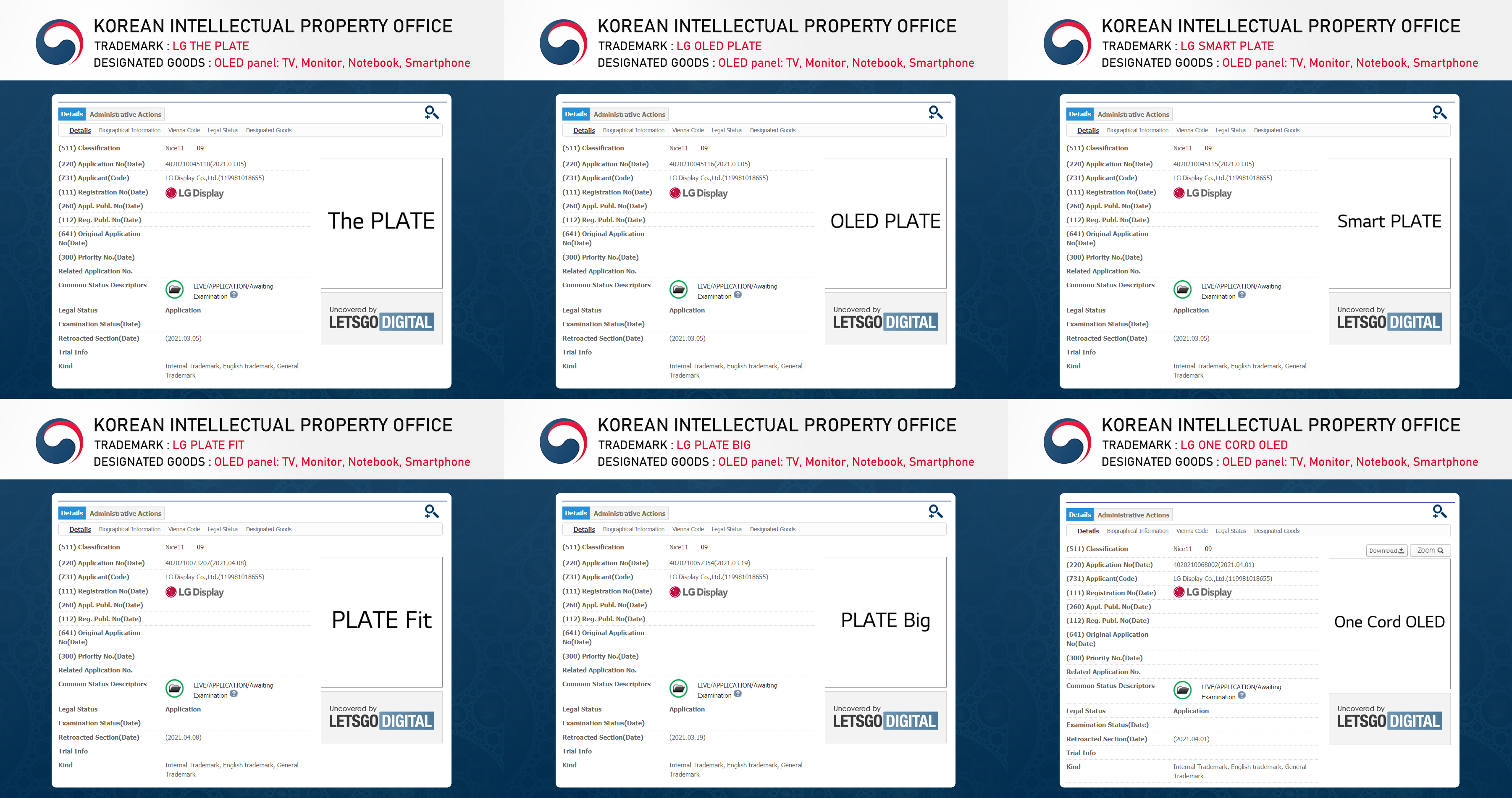
After the forerunner Panasonic who worked closely with LG Display, since 2020 LG Display offers an optional heatsink kit with their Oled panels. So far we have Toshiba, Sharp and Sony who use a heat sink in their Oled tv in addition to Panasonic.

https://av.watch.impress.co.jp/docs/...a/1269662.html

https://av.watch.impress.co.jp/docs/news/1319782.html


With a greater quantity of production of the new generation Olel panel (Evo), we will undoubtedly have more manufacturers next year with this option.
New generation of slab plus the option of heatsink structure, we will certainly have the best OLEDs produced to date.
I wasn't aware LG was using the Heatsink for their OLED panels or is this for sets outside the U.S. market.

Surprised Sony was the only one to combine the Heatsink and newer panels this year.
  Reply With Quote
Old 07-27-2021, 06:47 AM   #583
DDH DDH is offline
Senior Member
 
Aug 2020
Default

Samsung to launch much-anticipated QD-OLED TV, expand MicroLED lines
New technology launches are aimed at strengthening its TV market leadership

https://www.kedglobal.com/newsView/ked202107250002
  Reply With Quote
Thanks given by:
Robert Zohn (07-27-2021)
Old 07-27-2021, 08:16 AM   #584
DDH DDH is offline
Senior Member
 
Aug 2020
Default

MicroLED TV
https://www.microled-info.com/microled-tv

Quote:
One interesting thing to note is that while most so-called microLED TVs are indeed emissive displays, the actual LED chips inside these TVs are not always miicroLEDs, but sometimes actually mini-LEDs (this is true for example in Samsung's TVs, at least for the first-gen models).
  Reply With Quote
Thanks given by:
gkolb (07-27-2021), Robert Zohn (07-27-2021)
Old 07-27-2021, 09:30 AM   #585
DDH DDH is offline
Senior Member
 
Aug 2020
Default

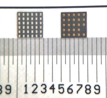
The World’s First 0.49mm Fine-Pitch Mini-LED Display Panel Using 36 Pixel-in-1 MiniLED πLED Package.

https://www.businesswire.com/news/ho...60;LED-Package.
  Reply With Quote
Thanks given by:
Robert Zohn (07-27-2021)
Old 07-27-2021, 09:39 AM   #586
DDH DDH is offline
Senior Member
 
Aug 2020
Default

Hands on: TCL 6-Series 2021 8K QLED TV review
The world’s cheapest 8K QLED TV has arrived

https://www.techradar.com/reviews/tc...021-8k-qled-tv
  Reply With Quote
Old 07-28-2021, 08:19 AM   #587
DDH DDH is offline
Senior Member
 
Aug 2020
Default

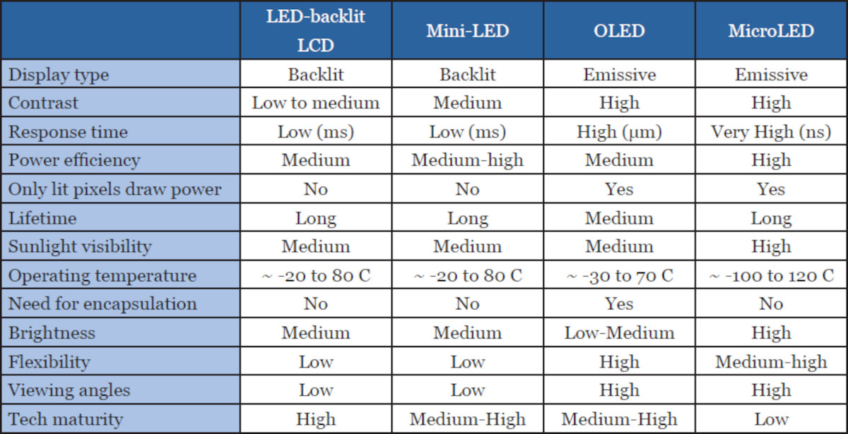
OLED vs MicroLED - a technology comparison

https://www.oled-info.com/oled-vs-mi...ogy-comparison
  Reply With Quote
Thanks given by:
gkolb (07-30-2021), Robert Zohn (07-28-2021)
Old 07-28-2021, 08:21 AM   #588
DDH DDH is offline
Senior Member
 
Aug 2020
Default

LG Display Reports Second Quarter 2021 Results
http://www.lgdisplay.com/eng/prcenter/newsView
  Reply With Quote
Thanks given by:
Robert Zohn (07-28-2021)
Old 07-28-2021, 08:23 AM   #589
DDH DDH is offline
Senior Member
 
Aug 2020
Default

LG Display’s large OLED, 8-year investment is about to pay off… "Realization of surplus in the second half"
https://www.etnews.com/20210728000127?mc=em_009_0001
https://translate.google.com/transla...0001&sandbox=1
  Reply With Quote
Thanks given by:
Robert Zohn (07-28-2021)
Old 07-28-2021, 10:58 PM   #590
Pagey123 Pagey123 is offline
Special Member
 
Apr 2020
Middle, TN USA
Default

So glad you got to see the new Sony stuff, Robert! Love your contributions to the AV enthusiast community here, as well as the YouTube collabs with FOMO, Keep It Classy, etc. You are the salt of the earth.
  Reply With Quote
Thanks given by:
Robert Zohn (07-29-2021)
Old 07-29-2021, 07:15 AM   #591
DDH DDH is offline
Senior Member
 
Aug 2020
Default

LG Display Says It Will Not Discard LCD Panel Business
http://www.businesskorea.co.kr/news/...ml?idxno=72941
  Reply With Quote
Thanks given by:
Robert Zohn (07-29-2021)
Old 07-29-2021, 08:30 AM   #592
DDH DDH is offline
Senior Member
 
Aug 2020
Default

As Innovative Micro LED Applications Emerge, Overcoming Mass Transfer and Testing Problems Is Top Priority
https://www.ledinside.com/node/32166
  Reply With Quote
Thanks given by:
Robert Zohn (07-29-2021)
Old 07-29-2021, 08:48 AM   #593
DDH DDH is offline
Senior Member
 
Aug 2020
Default

Quote:
Originally Posted by DDH View Post
Supertest OLED EVO LG 55G1 4K
"The first TV from LG Electronics, equipped with the new 'EVO' technology, brings with it tangible improvements in image quality, in the richness of shades - especially in low lights - as well as operating system, menus and some improved functions"

https://www.avmagazine.it/articoli/4...-4k_index.html

LG OLED 55G1 EVO pixel structure
Struttura pixel LG OLED 55G1 EVO - YouTube
The new OLED panel of LG EVO TVs

https://www.avmagazine.it/articoli/4...evo_index.html
https://translate.google.com/transla...evo_index.html
  Reply With Quote
Thanks given by:
Robert Zohn (07-29-2021)
Old 07-29-2021, 05:30 PM   #594
Lee A Stewart Lee A Stewart is offline
Blu-ray Baron
 
Lee A Stewart's Avatar
 
Jan 2019
Albuquerque, NM
Default

Panasonic's first OLED TVs with HDMI 2.1 are now available

https://www.flatpanelshd.com/news.ph...&id=1627546506
  Reply With Quote
Old 07-30-2021, 08:30 AM   #595
DDH DDH is offline
Senior Member
 
Aug 2020
Default

Quote:
Originally Posted by DDH View Post
LG Display’s large OLED, 8-year investment is about to pay off… "Realization of surplus in the second half"
https://www.etnews.com/20210728000127?mc=em_009_0001
https://translate.google.com/transla...0001&sandbox=1
LG Display's large OLED, 8-year investment is about to pay off... "Realization of surplus in the second half"
https://english.etnews.com/20210729200001?SNS=00001
  Reply With Quote
Thanks given by:
Robert Zohn (07-30-2021)
Old 07-31-2021, 11:47 PM   #596
DDH DDH is offline
Senior Member
 
Aug 2020
Default

QD-OLED TVs Expected in H122
https://www.oled-a.org/qd-oled-tvs-e...22_080221.html
  Reply With Quote
Old 08-02-2021, 01:42 AM   #597
DDH DDH is offline
Senior Member
 
Aug 2020
Default

DISPLAY DAILY

MicroLED Display: Road to Commercialization (Part 1)

Quote:
MicroLED display technology is making steady progress towards commercialization. The technology still faces several complex manufacturing challenges, which will take time to resolve. Display Week 2021, gave a glimpse of microLED technology developments by various companies to resolve the manufacturing issues.

MicroLED has the potential to outperform both LCD and OLED technologies in terms of color reproducibility, brightness, reliability and low power consumption. To compete with LCD (Quantum Dot & miniLED) and OLED in the consumer market, microLED products need to have zero defects, high performance, high uniformity, high volume scalability and cost competitive manufacturing. The success of commercialization and mass production will depend on the ability to scale up for volume production with competitive price performance.

Increasing Investments

According to Yole’s presentation at DisplayWeek 2021,

“more than 8900 MicroLED display patents have been already filed by 480 organizations. More than $5.1 Billion has already been spent on MicroLED. Start-ups raised more than $250 million in the last 18 months. Display makers dominate activity followed by start-ups. Chinese companies have been dominating activity (45%) and Korea came back strongly in 2020 (22%) driven by Samsung and LG. Samsung was most active in 2020, followed by CSOT, BOE, Visionox, Playnitride, Konka and Facebook. More than 50 prototypes of products have already been produced by more than 30 companies. Samsung has introduced a 4K 110-inch MicroLED TV (2021) but it costs $155K. Vuzix promised to ship the first AR device based on JBD (Jade Bird Display) MicroLED later this year”.

Complex Manufacturing

MicroLED is a self-emitting display consisting of arrays of microscopic LEDs each forming a pixel. It has a simple structure but a complex manufacturing process. The microLED supply chain consists of the following steps.

- GaN epiwafer LED creation
- Processing of thin film LEDs
- Mass transfer of the chips to the display backplane
- Inspection and repair processes

Display integration of MicroLED can be heterogeneous or monolithic integration. In the heterogeneous type, makers use pick and place process to make microLED arrays, and chips are transferred from an epiwafer or carriers to the display backplane (LTPS or Oxide TFT on a glass or flexible PI substrate). The monolithic integration process involves microLED array and backplane hybridization.


Source; Playnitride DisplayWeek 2021

Chip Manufacturing

Companies are developing solutions to reduce costs and remove roadblocks for MicroLED commercialization. Saphlux has developed NPQD technology that integrates an RGB pixel within one chip. This process can reduce total system costs. According to DSCC's microLED presentation, at Display Week 2021,

“Triad chip (RGB sub-pixels built into a single chip)(offered by Seoul Viosys),

-Pros: (a) reduced cost of mass transfer (b) larger chips: easier to handle during transfer/ repair.
- Cons: (a) with native colors: increase complexity and cost of the LED manufacturing (b) with color convertors: QD material costs.

Smartpixel (microLED bonded on Microdriver IC)

- Pros: removes the need for TFT backplane
- Cons: cost of CMOS wafer and hybridization”.

Color Conversion: The mass transfer process that requires bonding RGB (Red Green Blue) MicroLED to the display backplane accurately and efficiently is very challenging. Also different colors of LED need slightly different voltage and drive currents. Color conversion by Quantum Dots (QDs) (QDCC) or by phosphor provides another alternative. Using single-color (blue) MicroLED chips and color converting them with QD layers can help in the manufacturing process.

Nanosys’s presentation at DisplayWeek 2021 showed

“a breakthrough of new heavy metal free green QDCC emitter that delivers product ready brightness, color accuracy and reliability. The microLED size needs to be below 7 micron to be cost competitive in future displays."

According to the company its color-converted red provides 3.5x better performance at an economical cost, and is crucial for emerging display applications. AR requires ultrahigh efficiency and brightness. QDCC microLEDs at 1.8 microns can deliver the resolution and energy efficiency required for the future of AR.

Nanosys has acquired the microLED display company “glō” recently to accelerate MicroLED development & adoption.


Figure: 2 Source:Nanosys

Inspection, Repair & Yield

Manufacturing and yield problems can become issue in epitaxy, chip, mass transfer, bonding, driving technology, backplane, inspection and repair. The integration of in-process test, redundancy and repair are used to improve yield. Also as display resolutions gets higher, pixels are getting smaller: the trend is moving from 50 micron to 5 micron to 1 micron. This requires development of inspection tools that can achieve sub-micron resolutions. According to an InZiv presentation, it has built high-resolution inspection tools that can inspect any size microLED and analyze defects to improve processes and accelerate time to market. InZiv makes high-resolution tools for OLED and QLED also.

MicroLED companies also need to use mass testing and repair methods to reduce the cost and time of assembly. Companies such as Toray are working on equipment for microLED wafer inspection, repair and transfer. Laser repair equipment can remove defective microLEDs. As a presentation by DSCC on microLED session explained

“redundancy is an alternative way to reduce number of defective pixels. However, redundancy is expensive as it greatly increases LED consumption and the number of transfers. If the speed of the repair process is high enough, redundancy should not be required.“

Uniformity: microLED chips need wavelength uniformity and thickness uniformity for display applications. Solutions from MOCVD suppliers such as Aixtron, Veeco and others are helping to resolve issues caused be poorer uniformity. According to an Instrument Systems (Konica Minolta Group) presentation, the uniformity analysis of displays requires accurate color and luminance measurements. A combination of a highly accurate spectroradiometer and a fast RGB camera can provide a fast and accurate solution.

  Reply With Quote
Thanks given by:
Robert Zohn (08-02-2021)
Old 08-02-2021, 01:51 AM   #598
DDH DDH is offline
Senior Member
 
Aug 2020
Default

DISPLAY DAILY

MicroLED Display: Road to Commercialization (Part 2)

Quote:
In the first part of this article (MicroLED Display: Road to Commercialization Part 1, I covered investment, chip and LED manufacture and inspection repair and yield. Here, I'm covering mass transfer, supply chain development and the application market.

Mass transfer & Bonding

Mass transfer is critical for cost competitiveness with TFT-LCD and OLED.

- X Display Company (XDC) presented that mass transfer throughput and yield can be improved by using elastomer stamps. The company showed that for a 5.1" display, by using their PixelEngine and microICs, they are able to achieve functional sub-pixel yield of: red100%, green 99.996% and blue 99.998%. By using PixelEngine devices (microIC, RGB, All-In-One) they are able to increase mass transfer throughput. The company said elastomer stamp mass transfer is scalable using a conformable stamp with tunable short-range adhesion forces that achieved 99.99% transfer yields in R&D.
- Recent news from Electronics and Telecommunications Research Institute (ETRI) Korea showed that a new material, SITRAB adhesive, can be used to combine the transfer and bonding process into one process (applied homogenized laser to the SITRAB film attached to the MicroLED for a few seconds to develop the core process of simultaneous transfer and bonding). ETRI said this technology can reduce the high investment costs for transfer and bonding equipment and can also help to perform repair of defective pixels.
- Coherent recently announced its new UVtransfer integrated laser system that performs three processes in MicroLED fabrication: Laser Lift-Off (LLO), laser-Induced Forward Transfer (LIFT), and repair/trimming.
- Vuereal presented its Micro-Solid printing technology that can overcome the limitation to throughput and yield challenges.
- A collaboration of PlayNitride, Unimicron Corp (PCB backplane), and Macroblock (driver ICs) have shown the use of mass transfer of MicroLED onto a printed circuit board backplane, which can reduce production costs.
- Compound Photonics has developed its IntelliPix end to end microdisplay platform for AR/MR. The company presented that it is well positioned to extend IntelliPix’s benefits and pixel array design expertise to direct view displays.
X Display


Source; XDisplay Display Week 2021

Supply Chain Development

There are many different options and processes to resolve microLED manufacturing issues for commercialization. A supply chain ecosystem is proving difficult to develop for mass production because of the many underlying issues.

- There is no standard manufacturing solution for commercialization. Every firm has its own idea.
- Start-up companies are mostly fabless with licensing capabilities, and they need partnerships for manufacturing. Large established companies are reluctant to depend on a single start-up for their supply.
- Suppliers with LTPS-TFT capacity for backplane or other manufacturing capabilities need to invest capital for transfer, inspection/testing, and create a path to mass market.
- Panel suppliers and set suppliers need to be confident about profit margins for on-going business to allow them to invest capital.

More partnership and collaborations among panel makers, set makers and MicroLED chipmakers are required. Major display suppliers - Samsung, LGD, AUO, Innolux, BOE, Tianma, CEC Panda, Visionox and others are all increasing their activities in microLED display, which will help to establish supply chains for volume production.

Application Market

There are already many microLED demonstrations in different applications, such as large-size TV, automotive transparent display, flexible display, wearable devices and as AR/HUD display source.

- PlayNitride: has developed a selective mass addressable repair technology for lower cost. The company showed a 1.39" circular display for wearables and a 7.56" transparent display for photoframes as well as an 89" 5K ultra wide curved displays at DisplayWeek 2021.
- Royole: A microLED with ultra low aperture ratio and simple or non-encapsulation requirements, can lead to high stretchability, fine pitch and high transmittance. Using 90x 150 micron LEDs, a 2.7" 42 PPI RGB stretchable microLED panel was also demonstrated.
- Vuereal: its Micro-Solid Printing Technology has allowed the development of custom displays for niche markets such as high-brightness, high-transparency (>80%) display, wearable, and automotive. Samples will be available in Q4 2021.
- Jade Bird Display: announced the mass product of 0.13" monochrome microLED microdisplay panels and optical engines and assemblies. These products enable ultra-compact AR glass designs.
- AUO: received the best technology demonstration award at DisplayWeek for its integrated vehicle cockpit with microLED display after showing a 12" auto display, a 10.4" transparent display and a 1.4" round MicroLED display panel.

Companies are initially targeting digital signage, public display, AR/VR, wearable, and automotive (HUD) applications.

In Conclusion

High-speed transfer, assembly technologies, yield and defect management need to improve and supply chains need to be established before large volume commercialization in consumer products can be done. In the meantime, suppliers will focus on markets with higher priced, lower volume, value-based products.
  Reply With Quote
Thanks given by:
Robert Zohn (08-02-2021)
Old 08-02-2021, 02:36 AM   #599
DDH DDH is offline
Senior Member
 
Aug 2020
Default

'Samsung Display focusing on securing uniformity in QNED panel'


Quote:
Tech has ‘best characteristics’ for display, UBI Research says


Samsung Display was currently focusing on securing the screen uniformity of its quantum dot nanorod LED (QNED) display panel, as it wraps up development, market research firm UBI Research said on Friday.

The research firm unveiled core patents filed by Samsung Display it found, which shows the structure of QNED display panels.

According to UBI Research, QNED display panel stacks quantum dot (QD) and color filter __ the color conversion layers __ as well as the nanorod LED on top of the thin-film transistor (TFT). QNED’s TFT shares the same 3T1C, or 3 transistors and 1 capacitors, used in large OLED panels.

The difference between QNED and OLED is that, while OLED has the electrodes, both cathode and anode, and the electrode line located on top of and below the light emitting materials, QNED has the pixel electrodes and electrode lines located on the same plane, the research firm said.

QNED also has an additional reflective electrode to increase efficiency of light output. Pixel electrodes also acts as alignment electrodes for the nanorod LED, UBI Research said.

UBI Research explained further: In a QNED pixel, multiple pixel electrodes are also connected serially. Nanorod LEDs are positioned between these pixel electrodes. These pixel electrodes are also on the pixel walls made out of insulating materials. Each pixel is surrounded by banks to separate regions.

The core technologies in QNED that were noticeable were those for driving and sensing, the research firm said.

Samsung Display’s QNED includes driving techniques for aligning the nanorod LEDs and uniform pixel controls for ones with different number of naonorod LEDs.

The alignment circuit has switching devices for each pixel. These switching devices sends a signal on the alignment status to the pixel. These signals sent by pixels determine how nanorod LEDs are aligned.

On the circuit, there are transistors that approve these signals and sensing transistors that can check the alignment of the nanorod LEDs. These sensing transistors check the number of nanorod LEDs by analyzing the electric currents on the pixels.

Ultimately, after these processes, the panel supplies current to each pixel so that the luminance is uniform across the entire screen, even if the number of nanorod LEDs on each pixel are different. The current sent for each pixel is based on the data analyzed by sensing transistors.

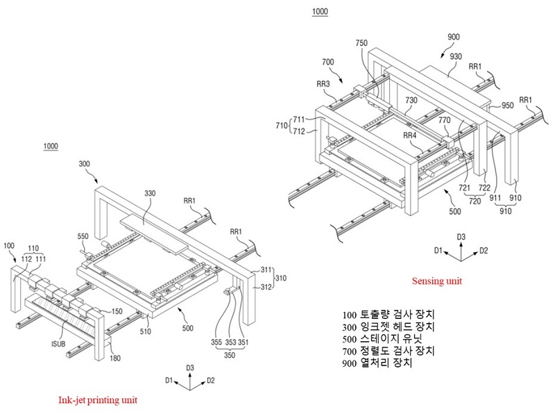
There are also sensing technologies used in the production of QNED panels. During the inkjet process during production, these technologies sense the number of nanorod LEDs in the ink, the viscosity of the solvent, the number of nanorod LEDs sprayed on the substrate and their alignment state.

“The reason Samsung Display is developing QNED as part of its large-size display business, is that it is the only display that can produce the image quality that Samsung Display's biggest customer, Samsung Electronics, can satisfy,” UBI Research noted.

Samsung Electronics' TV business is aiming to use QD to make color gamut better than OLED, and to use a display that can maximize HDR performance with high luminance and excellent gradation characteristics on a bright screen, the research firm added.

“It can be confirmed” by the structures UBI Research analyzed that QNED is the display with the best characteristics, the firm claimed.

https://twitter.com/DDBH59/status/1422021123206746112

Last edited by DDH; 08-02-2021 at 03:04 AM.
  Reply With Quote
Old 08-02-2021, 04:20 AM   #600
DDH DDH is offline
Senior Member
 
Aug 2020
Default

QNED (quantum dot nano-rod LED) structure and core technology

https://olednet.com/210729-2-2/
https://translate.google.com/transla...2%2F&sandbox=1
  Reply With Quote
Reply
Go Back   Blu-ray Forum > 4K Ultra HD > 4K Ultra HD Players, Hardware and News


Posting Rules
You may not post new threads
You may not post replies
You may not post attachments
You may not edit your posts

BB code is On
Smilies are On
[IMG] code is On
HTML code is Off

Forum Jump


All times are GMT. The time now is 09:35 PM.